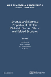
Structure and Electronic Properties of Ultrathin Dielectric Films on Silicon and Related Structures
With the ever-decreasing dimension, laterally and vertically, in CMOS and DRAM technology, the understanding of thin insulators and their interfaces with silicon have become of critical importance. As a result of this scaling of semiconductor devices, an increased interest from industrial, government, and university laboratories has become evident in this field of study. The book, first published in 2000, includes detailed theoretical studies of the nature of SiO2 and its interface with silicon, electron paramagnetic resonance for the study of defects, electron tunneling, and band alignment among others. There are also studies developing new techniques and advancing our understanding of these dielectrics and interfaces, including addressing the issue of dielectric breakdown. Aside from the work addressing SiO2, there are a number of papers regarding the application of the so-called 'high-k' dielectrics. The high-k materials addressed in the volume include such films as Ta2O5, HfO2, Bi2Ti2O7, CeO2, and ZrO2.
Product details
June 2014October 2000
Paperback
9781107413320
404 pages
229 × 152 × 21 mm
0.54kg
Available

