Transistor Scaling
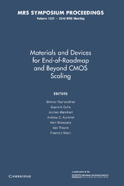
For the past four decades, geometric scaling of silicon CMOS transistors has enabled not only an exponential increase in circuit integration density - Moore's Law - but also a corresponding enhancement in the transistor performance. Simple MOSFET geometric scaling has driven the industry to date. However, as the transistor gate lengths drop below 35nm and the gate oxide thickness is reduced to 1nm, physical limitations such as off-state leakage current and power density make geometric scaling an increasingly challenging task. In order to continue CMOS device scaling, innovations in device structures and materials are required and the industry needs a new scaling vector. Starting at the 90 and 65nm technology generation, strained silicon has emerged as one such innovation. Other device structures such as multigate FETs may be introduced to meet the scaling challenge. This book shares results and physical models related to MOSFETs and to discuss innovative approaches necessary to continue the transistor scaling. Expanded versions of presentations in the areas of technology development are featured
Product details
November 2006Hardback
9781558998698
205 pages
228 × 152 mm
0.432kg
Available

